Key research area "Optolelectronics and Photonics"
The research within the profile area Optoelectronics and Photonics is focussed on the physics and applications of optical technologies.
It is driven by innovative concepts from quantum optics, coherent optics, ultrafast nanooptics and optoelectronics. The goal of the coordinated research is to establish novel information technologies based on nonlinear light-matter interactions and quantum effects.
Within the experimental research new materials are developed and functional nanostructures as well as photonic quantum devices are produced and evaluated. The theoretical work covers the full range from atomistic material description and quantum optics to protocols for quantum information processing.
The area of applications is dominated by research in the field of automotive lighting. Together with the L-Lab, the industrial development of prototypes and technology demonstrators is performed.
The interdisciplinary cooperation in the profile area "Optoelectronics and Photonics" is supported by the Collaborative Research Center TRR 142. Among the participating scientists are Leibniz Prize and ERC Grant winners.
Contact: Prof. Dr. Thomas Zentgraf
Research areas involved: Physics, Electrical Engineering, Chemistry, Mathematics, Computer Science
Selected Research Projects
When a sufficient number of quantum particles are interconnected, quantum computers can handle tasks that are unsolvable for classical computers. This – among other unique selling points – is a major advantage of photonic platforms: Integrated architectures and sophisticated manufacturing processes offer an enormous scaling potential. The aim of the PhoQuant joint project is to develop a purely photonic quantum computer, based on Gaussian Boson Sampling (GBS), with at least 20 (after 2.5 years) or 100 (after 5 years) individually controllable channels. In addition to the development of a programmable GBS QC demonstrator with application-relevant algorithms, the implementation of a user interface as an interface for industrial and academic users is in the foreground.
In the subproject Quantum Computing Test Platform (PhoQuant-QCTest), essential components, including an optimized integrated squeezed light source and functionalities such as coherent displacement and homodyne detection, and algorithms for the demonstrator will be developed. Furthermore, an experimental test platform will be provided to test the developed components and algorithms under realistic conditions before transferring them to the demonstrator. The components developed by project partners based on the new material system thin-film lithium niobate on insulator (LNOI) will also be evaluated with the help of the test platform. New and known GBS QC algorithms are verified by means of information-theoretical complexity investigations.
Seven research groups of the Institute for Photonic Quantum Systems (PhoQS) with complementary expertise are performing the subproject PhoQuant-QCTest.
The joint project PhoQuant is funded by the German Federal Ministry of Education and Research (BMBF) in the period from 01.01.2022 to 31.12.2026 and combines the expertise of 14 partners from academia and industry.
Further information can be found here.
Scientific contact:
Prof. Dr. Christine Silberhorn
Quantum technologies are expected to have a transformative impact by exploiting fundamental quantum mechanical effects for technological applications. Photons are the only reliable qubit for quantum information transmission, making them an essential resource for quantum technologies. However, quantum photonics will only meet its expectation as a ground breaking technology when integrated in a scalable fashion. The project will demonstrate that the thin film lithium niobate on insulator platform can simultaneously link all quantum photonics building blocks on a single platform, resulting in fully integrated quantum photonic integrated circuits. This will result in the first compatible integration platform hosting semiconductor quantum emitters, quantum memories based on rare-earth ions, cryogenic electronics, and superconducting single-photon detectors together with the outstanding properties of CMOS-compatible lithium niobate on insulator: low-loss circuits and fast modulators. LiNQs will lay the foundation for Europe’s forefront position in a future photonics-driven quantum technology industry.
This project is funded by the European Research Council (ERC) under the European Union's Horizon 2020 research and innovation program (Grant Agreement No. 101042672).
Research contact: Prof. Dr. Klaus Jöns
Further information: https://cordis.europa.eu/project/rcn/208461/factsheet/en
Superconducting detectors are the gold-standard measurement tools for measuring single photons. They offer unprecedented efficiency, signal-to-noise ratio, and timing accuracy. As single devices, these detectors alone have already revolutionised the field of quantum optics, and are beginning to be used for remote sensing, communication in space, and even the search for dark matter.
The frontier of this technology is to build arrays of these detectors, for use in imaging and large-scale photon counting systems. Key to exploiting the performance of these devices is to optimise their underlying quantum response function. This is achieved by characterising and engineering the devices through a process called quantum detector tomography. The aim of QuESADILLA is to perform this characterisation and optimisation on a range of different degrees of freedom on arrays of superconducting detectors. In this way, these detectors will not only count photons, but also provide spectral, spatial and temporal information of the optical states they are measuring. This approach has applications in high dynamic range imaging, spectrally-broadband optical sensing at the single photon level, and high dynamic range photon counting.
This project will employ and equip a team of three scientists over a period of five years, who will develop the fabrication and characterisation tools required for building arrays of superconducting detectors.
Through the project, three scientists will be employed and equipped to develop fabrication and characterization tools to build the arrays of superconducting detectors for five years.
This project is funded by the European Research Council (ERC) under the European Union's Horizon 2020 research and innovation program (Grant Agreement No. 101042399).
Research contact: Prof. Dr. Tim Bartley
Further information: https://cordis.europa.eu/project/rcn/208461/factsheet/en
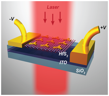
Understanding nonlinear optical properties of two-dimensional semiconductors and their heterostructures is essential for a successful design and fabrication of high-performance nanophotonic devices. In particular, for all-optical photonic elements, nonlinear properties need to be precisely controlled and combined with sophisticated functionalities. Such functionalities can be provided be nano-patterned materials, also known as metasurfaces or metamaterials. The local electromagnetic fields induced by metamaterials can be few-orders higher than the mean value of the external illumination field. The project funded by the ERC through the Consolidator Grant “NONLINMAT” focusses its research on the combination of the significantly enhanced electromagnetic fields from nano-patterned metamaterials with semiconductor quantum wells in Gallium Nitride and atomically thin transition metal dichalcogenides like monolayers of Tungsten- or Hafnium-Disulfide (also called 2D materials).
Besides, distinct from the conventional bulk and quasi-2D semiconducting materials, quantum confinement and reduced dielectric screening in 2D semiconductors remarkably enhance quasiparticle interactions and result in large binding energies of excitons, where many-body effects need to be considered. In such a system of 2D semiconductors, investigations of many-body physics become a very exciting research field for exploring the fundamentals of quantum mechanics. In particular, high-order unconventional excitonic quasiparticles can exist such as trions and biexcitons, and the enhanced electromagnetic fields of laser excitation may help for observations of these high-order quasiparticles and reveal the underlying many-body effects. On the other hand, nonlinear optical properties of nano-patterned metamaterials can be modulated by atomically thin 2D materials. The possible localized surface resonances of nanostructures occur at the metal-2D semiconductor interfaces. Moreover, by adjusting the frequency bands of nanostructures overlapping with the emission bands of the 2D material, the resonant coupling of emission bands may result in new physics, such as valley-polarized surface plasmons.
The project studies the influence of selective coupling mechanisms based on symmetry aspects of the nanostructures and the lattice symmetry of the 2D materials. The focus is hereby on the enhancement of nonlinear optical effects and the control of properties purely with light. The findings will lead to a deeper understanding of coupling mechanisms between artificially engineered nanostructures and natural material systems. The improved light-matter-interaction, on the other hand, can result in smaller and more efficient all-optical devices for future applications in quantum information processing.
This project has received funding from the European Research Council (ERC) under the European Union’s Horizon 2020 research and innovation programme (grant agreement No. 724306).
Research contact: Prof. Dr. Thomas Zentgraf
Further information: https://cordis.europa.eu/project/rcn/208461/factsheet/en
One of the most prestigious grants for international top-level research is the “ERC Consolidator grant”, with which the European Research Council awards excellent young scientists who already pioneered their field with visionary projects.
In 2016 the physicist Christine Silberhorn was awarded by the ERC for her project “QuPoPCoRN-Quantum Particles on Programmable Complex Reconfigurable Networks”, which started in July 2017. Since then Prof. Silberhorn and co-workers investigate the complex interactions and dynamics of multiple quantum particles within large networks, an extremely challenging task.
But doing so reveals the underlying structure of an enormously diverse range of phenomena. Therefore, a reliable platform to investigate complex quantum network dynamics, which incorporates the rich interplay between noise, coherence and nonclassical correlations, will be an extremely powerful tool. The scientists develop time-multiplexed optical networks, in combination with tailored multi-photon states as a new platform for large-scale quantum networks. This approach allows them to emulate multi-particle dynamics on complex structures, specifically the role of bosonic interference, correlations and entanglement. To achieve the required large networks sizes, novel decoherence mitigation strategies must be developed: programmable noise, topologically protected quantum states and perpetual entanglement distillation.
The objectives in QuPoPCoRN target the overall goal to understand the role of multi-particle quantum physics in complex, large-scale structures harnessing time-multiplexed photonic networks.
This project has received funding from the European Research Council (ERC) under the European Union’s Horizon 2020 research and innovation programme (grant agreement No. 725366 ).
Contact: Prof. Dr. Christine Silberhorn
The project "UNIQORN" (Affordable Quantum Communication for Everyone) started at the end of 2018 within the framework of the European research initiative "Quantum Flagship". The goal of the three-year project is to use photonic technologies in quantum communication. The optical systems, which currently require structures of the order of meters, will in future be accommodated on millimeter-sized chips. In addition to reducing the size and thus the cost, such systems are robust and can be reproduced better.
"UNIQORN" is a collaborative project with partners from industry and universities. 17 groups from various European countries work together under the coordination of the "Austrian Institute of Technology". In Paderborn special nonlinear integrated optical devices (e.g. photon-pair sources) will be developed, which contribute significantly to the desired miniaturization. These devices are then implemented by other project partners into hybrid functional units and then used to demonstrate the functionality for selected quantum applications in real-world communication networks.
The UNIQORN project receives funding from the European Union's Horizon 2020 research and innovation programme under grant agreement No. 820474.
Contact: Prof. Dr. Christine Silberhorn
Further information: https://quantum-uniqorn.eu/
Data security is critical to our modern society. Because of threats ranging from personal data and identity fraud to cyber attacks that threaten the integrity of sovereign nations, the need for secure communications and computing has never been greater. In theory, quantum networks would address these problems because they are demonstrably secure for cryptographic communication tasks. The next step now is to build physical quantum networks that implement such secure communications in practice. PhoQSNet, our proposal under the Large Devices Initiative, will provide the infrastructure and technology needed to build a network for photonic quantum systems at the urban scale.
The ambitious goal of PhoQSNet is to provide the infrastructure for a three-node quantum network. This will allow us to explore various configurations of quantum communication technology, including point-to-point protocols, quantum relays, and quantum repeater nodes. In doing so, we will explore protocols that use both discrete and continuous coding of quantum information.
The physical fiber network will connect buildings A and P on the main campus of the University of Paderborn with the Heinz Nixdorf Institute, located 3.6 km away. All three sites will be connected with commercial dark fiber from the city's standard fiber network. Each of the three nodes will host a quantum transmitter and receiver station equipped with complementary components to implement various quantum communication protocols: Quantum light sources and detectors, and instruments to characterize quantum and classical channels. The modular structure of PhoQSNet ensures future compatibility with novel fiber-based quantum communication technologies. Our presented test network is therefore a key enabler for quantum communication applications.
Our initiative is based on an established collaboration between electrical engineering, physics, mathematics and computer science, which has been brought together in the recently founded Institute for Photonic Quantum Systems at the University of Paderborn. Thus, our initiative has expertise in all relevant areas of the project, as well as an established umbrella organization for its implementation and long-term sustainability. This unique interdisciplinary research environment, with specialists in quantum sources and detectors, high-speed communication systems, and codes and cryptography, enables us not only to implement existing interdisciplinary projects, but also to establish groundbreaking future research directions and ensure the continued existence of PhoQSNet well beyond the first funding phase for years to come.
From PhoQS, the research groups Hybrid Quantum Photonic Devices, Integrated Quantum Optics, Mesoscopic Quantum Optics and Circuit Technology are significantly involved in PhoQSNet. The project is funded by the DFG since 2022 over a period of five years. For more information, please visit the DFG project page.
Contact: Prof. Dr. Klaus Jöns
Within the Quantum Flagship, one of the largest and most ambitious research initiatives of the European Union, the project „Sub-Poissonian Photon Gun by Coherent Diffusive Photonics“, in short PhoG, is one of only 20 funded proposals in the first phase.
Phog consists of five partners from UK, Germany, Belarus and Switzerland, among them the “Integrated quantum optics group” of Prof. Silberhorn in Paderborn. Under the leadership of Natalia Korolkova from the University of St. Andrew the consortium will develop deterministic and compact sources for non-classical photonic states, the so-called Photon-Guns. To this aim they will engineer the losses and couplings in integrated waveguide arrays. These innovative devices will then be applied in metrology and other quantum technology tasks, e.g. to enhance the frequency stabilization of atomic clocks. The contribution of the partner in Paderborn will focus on the characterization of the non-classical states of light.
The PhoG project receives funding from the European Union's Horizon 2020 research and innovation programme under grant agreement No. 820365.
Contact: Prof. Dr. Christine Silberhorn
Further information: https://www.st-andrews.ac.uk/~phog/
Exponentially growing data traffic around the world leads to increasing demand for high speed server communication in data centers. Future communication systems have to reach data rates well beyond 100 Gbits/s and low power dissipation is becoming an increasingly important characteristic. Therefore, novel transceiver concepts are required to enable efficient high speed communication between servers. Silicon photonics enable high cost- and power-efficiency through integration of optical and electrical devices on a single chip, but data rates are limited by the small bandwidth of optical modulators in silicon technology. In the NyPhE project we investigate a new modulation concept to overcome the bandwidth limitations of silicon photonics transmitters. By means of sophisticated signal processing a bandwidth which is at least 3x the bandwidth of the silicon photonics optical modulators shall be achieved.
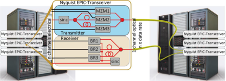
The main goal of the NyPhE project is the development of high speed electro-optical transceivers for data rates up to 400 Gbit/s. The basic approach to reach these data rates, is to make use of sequentially modulated and added Nyquist pulses. Due to their rectangular frequency spectrum, sequentially added Nyquist pulses do not influence each other and intersymbol interference is avoided.
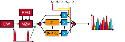
The rectangular spectrum is approximated by a frequency comb (see fig. 2a) which is generated by a MZM with a RF signal and a CW laser input. The optical signal is split into several channels, delayed and modulated by MZMs separately (see fig. 2b). Afterwards the modulated signals are combined and send to the receiver (see figure 2c). Thus, only a fraction of bandwidth is needed in each modulator. In the receiver, the signal is split up into channels again. Each channel signal is multiplied with a Nyquist pulse and demodulated in a BR. Afterwards the channel signals are amplified and converted into a serial signal.
The NyPhE project is funded by the Bundesministerium für Bildung und Forschung (BMBF). Our project partners are the Institut für Hochfrequenztechnik TU Braunschweig under the direction of Prof. Dr. Thomas Schneider, the Institut für Hochfrequenztechnik TU Dresden under the direction of Prof. Dr.-Ing. Kambiz Jamshidi, Sicoya GmbH and Leoni AG.
Research contact: Prof. Dr.-Ing. Christoph Scheytt
Further information: https://www.hni.uni-paderborn.de/en/sct/projects/nyphe/
The focus of the new potential area "Photonic Quantum Computing PhoQC" at Paderborn University is the implementation of important applications of quantum computing based on photonic quantum systems.
In the future, a nationally and internationally visible and leading research center in the field of photonic quantum computing will be created. Scientists from the faculties of natural sciences, electrical engineering, computer science and mathematics are involved in the initiative, mainly from the department of physics, the institute of computer science and electrical engineering and from the two areas of applied and pure mathematics.
The ambitious goal of this project can only be successfully pursued in a long-term and innovative interdisciplinary approach that combines the relevant disciplines in all research and development phases. The implementation of a viable concept for the promotion of young scientists is also of particular importance to anchor quantum technologies in society in the long term and to train excellent specialists for the economy of the future.
The targeted merger of complementary core competencies opens the future-oriented research field of photonic quantum computing and creates new synergies far beyond the capacities of the individual fields. Of particular importance in the German research landscape is the establishment of new structures that transfer the topic from basic research in physics to research activities in engineering.
The potential area of photonic quantum computing bundles expertise from Paderborn University in the profile areas "Intelligent Technical Systems" and "Optoelectronics and Photonics". The additional structures created within this project will help to further strengthen both profile areas professionally and to further advance the promotion of young people and equality in this research field, in which women have been far underrepresented to date. This project goes well beyond the existing profile areas by opening the new, visionary field of photonic quantum computing and bringing together areas from natural and engineering sciences as well as computer science and mathematics.
With the Research Center Photonic Quantum Computing, the research landscape in the field of quantum technologies and quantum computing is significantly expanded and strengthened in NRW and important structures for the interdisciplinary training of university graduates who have tailor-made expertise for the future field of quantum technologies.
The project is funded by the Ministry of Culture and Science of the State of North Rhine-Westphalia for the period from 01.11.2021 to 31.10.2024.
Contact: Prof. Dr. Christine Silberhorn
The aim of this project is the integration and application of high-efficiency superconducting detectors on nonlinear lithium niobate waveguides. This will enable to development of new tools in quantum optical communication technology. The main challenge is to maintain the advantages of the high nonlinearity of lithium niobate at the cryogenic temperatures required to operate the superconducting detectors, as well as ensure that the processing steps for each technology are mutually compatible. We have already made the first steps towards these goals in isolation; the new and exciting aspect of this project is to combine these functionalities on a single device, in order to realise the full potential of this technology. To do so, we combine the weald-leading lithium niobate waveguide fabrication at Paderborn University with the superconducting detector technology from the National Institute for Standards and Technology (NIST) in Boulder, Colorado. We plan to build five tailor-made modules to demonstrate the versatility of the the integrated superconducting optoelectronic platform. This comprises optimising the material properties of lithium niobioate waveguides with the thin-film superconductors required for the detectors. Each of these components will be designed such that it may be included as part of a wider quantum communication system, which can interconnect with other devices based on other platforms, for example single photon sources from single emitters. This modular approach, whereby the optimisation can be carried out on a component-by-component basis, is essential for the proliferation of quantum technology. The long-term vision is that this approach adds significant value and enables a broad functionality for quantum communication technology.
Research contact: Jun.-Prof. Tim Bartley
Weitere Informationen: https://www.photonikforschung.de/projekte/quantentechnologien/projekt/isoqc.html
Quantum technologies will have a transformative impact on our society; in particular, quantum computing which uses the fundamental quantum mechanical effect of entanglement to efficiently compute tasks that cannot be performed by a classical computer in realistic time. Together with superconducting quantum states (qubits), photons are the only platforms that have already demonstrated such a quantum advantage.
However, quantum photonics will only fulfill its expectations as a breakthrough technology if it is integrated in a scalable manner. The solution lies in quantum photonic integrated one-way quantum computing circuits, in which entangled photon cluster trains are used to encode and process quantum information on a compact photonic circuit.
In this project, the University of Paderborn will realize an integrated photonic circuit that enables this feed-forward operation thanks to ultra-fast integrated modulators and cryogenic electronics. Thanks to the thin film lithium niobate on insulator (LNOI) platform, which has a large electro-optical effect, low transmission losses in a wide wavelength range, as well as strong nonlinearity, it is possible for the University of Paderborn to realize all qubit manipulation operations of a one-way quantum computer on a single material platform. Connecting all one-way quantum computing devices simultaneously on a single material platform ensures high compatibility and enables efficient scalability. The University of Paderborn is thus developing the core technology for the realization of the first scalable, integrated one-way quantum computing demonstrator QPIC-1.
In the term from 01.09.2021 to 31.08.2025 the project is funded by the German Federal Ministry of Education and Research (BMBF). For further information please visit the BMBF project page.
Contact: Prof. Dr. Klaus Jöns
Metallic Nanowires II - Metallic nanowires on the atomic scale: Electronic and vibrational coupling in real world systems
Ideal one-dimensional electronic systems have peculiar properties, such as quantization of conductance, charge-density waves, and Luttinger liquid behavior, a variety of instabilities with a wealth of associated phase transitions.
These are due to their reduced dimensionality and the concomitant high electronic correlations. The exploration and identification of physical scenarios with one-dimensional properties under explicit consideration of 2D and 3D coupling is the central topic of the delocalized Research Unit FOR1700, where the Schmidt group collaborates with researchers from Würzburg, Duisburg, Berlin, Rome, Hannover, Gießen, Chemnitz, Düsseldorf, and Osnabrück.
Research contact: Prof. Dr. Wolf Gero Schmidt
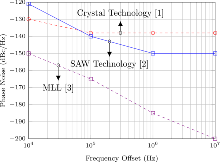
Low jitter signal sources are in widespread use for object detection, navigation systems, and ultra-high speed data communication systems. The jitter of the signal sources is dominated by the reference signal source which is a Surface Acoustic Wave (SAW) or a quartz oscillator. While these reference oscillators are standard for communication systems, the optical pulse train generated by a Mode Locked Laser (MLL) can have a better jitter performance by 2-3 orders of magnitude. It has also been shown that by using an electro-optical locking scheme, a microwave signal can be locked to an MLL [4]. Such Opto-Electronic Phase Locked Loops (OEPLL) have a great potential for a new class of low jitter frequency synthesizers.
The main drawbacks of these OEPLLs are their bulky and expensive optical components. Electronic-photonic integrated circuits based on silicon photonics technology offer the potential for extreme miniaturization of these optical components as well as integration of optics and low cost.
The goal of this project is to implement a monolithically integrated OEPLL with extremely low phase noise. In cooperation with our project partners at the Ruhr University of Bochum, we develop the next generation of low jitter microwave signal sources. This type of signal source employs a PLL that uses an MLL as a reference. In order to fully take advantage of the reference signal in the optical domain, the phase detection is done electro-optically using a Mach-Zehnder Modulator (MZM).
In the first phase, the whole system will be implemented using modular components. In the second phase, the MZM and the electronics will be integrated into a single silicon chip. The work is accompanied by theoretical investigation which will be validated by measurements.
The additive jitter of the OEPLL is expected to be less than the reference MLL jitter. The microwave signal then would have an in-band jitter which surpasses conventional electronic PLLs.
References:
[1] Kim et al, “Sub-100-as timing jitter optical pulse trains from mode-locked Er-fiber lasers,” Optics letters, vol. 36, no. 22, pp. 4443-4445, 2011.
[2] “Ultra Low Phase Noise Oven Controlled Crystal Oscillator,” Vectron, Datasheet OX-305.
[3] “Voltage Controlled SAW Oscillator Surface Mount Model,” Synergy Microwave, Datasheet HFSO1000-5.
[4] Jung et al, “Subfemtosecond synchronization of microwave oscillators with mode-locked Er-fiber lasers,” Optics letters, vol. 37, no. 14, pp. 2958-2960, 2012
Research contact: Prof. Dr.-Ing. Christoph Scheytt
The Priority Programme “Electronic-Photonic Integrated Systems for Ultrafast Signal Processing” (SPP 2111) is a research programme in the emerging field of integrated electronic-photonic systems using novel nanophotonic/nanoelectronic semiconductor technologies. The programme is funded by the Deutsche Forschungsgemeinschaft (DFG) and coordinated by Prof. Christoph Scheytt from Heinz Nixdorf Institute, Paderborn.
The overall objective of the Priority Programme is to address nanophotonic/nanoelectronic technology from a system perspective by investigating fundamental electronic-photonic signal processing concepts, algorithms, and novel integrated system architectures using predominantly photonic processing. The research is focused on three core areas which pertain to:
- Ultra-broadband electronic-photonic signal processing with bandwidth far beyond electronic bandwidth
- Frequency synthesis as well as high-speed data converters enabled by ultralow-jitter femto-second-pulse-lasers
- Optical/THz sensing.
The research is carried out in interdisciplinary cooperation between groups from semiconductor physics, electronics and photonics circuit and system design, computer science, communication engineering, microsystem technology, and sensors.
Research contact: Prof. Dr.-Ing. Christoph Scheytt
More information as well as a list of the funded projects of the first phase of the SPP (2018 - 2021) can be found on the DFG project data base GEPRIS: gepris.dfg.de/gepris/projekt/359861158 .
Fast digital-to-analog converters (DAC) are indispensable components for modern signal processing systems. Bandwidth and effective number of bits (ENOB) are important metrics for the performance of DACs. At the same time, those parameters constitute a trade-off in the design of a DAC: The more broadband the DAC, the less typically the ENOB. This is due to clock signal jitter limitations as well as linearity limitations of utilized transistors [1]. These fundamental, physical limitations motivate the search for new DAC concepts. To our opinion the most promising approach is presented by electronic-photonic DAC concepts and its integration by means of silicon photonics.
The goal of PONyDAC project is the investigation of electronic-photonic DACs based on optical time-interleaving and broadband optical pulse synthesis which can be implemented in modern silicon photonics technology through monolithic co-integration of photonic and electronic components on the same substrate. This novel approach has the potential to multiply today`s DAC bandwidths.
The functional principle is shown in figure 1. A Mach-Zehnder modulator (MZM) is fed optically by a continuous wave laser (CW) and driven electronically by a low noise radio frequency generator (RFG). By tuning both the amplitude and frequency of the drive signal as well as the MZM`s bias voltage one can generate precise, periodic Nyquist pulses with adjustable repetition rate and FWHM. In a following optical power splitter the Nyquist pulse train will be distributed into N arms and delayed in phase in respect to each other. MZMs located in those arms are driven by electronic DACs and modulate the light signals in the respective arms according to the digital input [ ]. The optical pulses are then combined by an interferometric structure with matching phase relation.
The concept of optical time-interleaving allows for a very high output signal bandwidth, which is a multiple of the bandwidth of state-of-the-art DACs. In the project an electronic-photonic DAC will be realized in modern silicon photonic technology, which targets for a DAC bandwidth of more than 100 GHz.
The PONyDAC project is funded by the Deutsche Forschungsgemeinschaft in context of the priority program „Electronic Photonic Integrated System for Ultrafast Signal Processing (SPP2111) “. Our project partner is the Institut für Hochfrequenztechnik TU Braunschweig under the direction of Prof. Dr. Thomas Schneider.
References:
[1] M. Khafaji, J. C. Scheytt, et. al., "SFDR considerations for current steering high-speed digital to analog converters," 2012 IEEE Bipolar/BiCMOS Circuits and Technology Meeting (BCTM), Portland, OR, 2012
[2] M. A. Soto et al., “Optical sinc-shaped Nyquist pulses of exceptional quality,” Nat. Commun., vol. 4, no. May, pp. 1–11, 2013.
[3] L. Zimmermann et al., “BiCMOS Silicon Photonics Platform,” Opt. Fiber Communication Conference (OFC), San Diego, p. Th4E.5, 2015.
Research contact: Prof. Dr.-Ing. Christoph Scheytt
Today’s society is based on the fast access to information. Getting a head start on information is key in business, finance, politics and security. Most of our information exchange is done via the internet. However, not only has the current structure of our internet limits in capacity but also data transfer is not secure. Therefore, we are in need to invest in a future network, capable of handling the massive data flow and allowing for secure data communication. Physics offers a solution to this difficult task in the so-called quantum internet. By using quantum mechanics, it is possible to encode information on the smallest quantum of energy, a single light particle called photon. Information encoded on single photons cannot be eavesdropped without the sender and original receiver noticing it. The basic concept relies on network nodes and special links, which are the quantum mechanical analogue to classical fiber amplifiers currently used to overcome transmission losses in standard network, to connect physically separated nodes with each other. However, the same quantum mechanical principle (non-cloning theorem) which makes the network totally secure also renders classical signal amplification impossible. Qurope develops quantum communication links taking advantage of another quantum mechanical effect to overcome transmission losses: Entanglement swapping using quantum repeaters. This allows transferring quantum information without physically sending a single information carrier the full distance to the receiver. Realizing such quantum repeaters requires quantum memories and entangled photon pair sources. The goal of Qurope is to develop a hybrid quantum repeater architecture based on dissimilar quantum systems and to test its performances in real-word applications. The envisioned implementation is based on two disruptive technologies that will be pioneered during the project: (i) Near-ideal quantum-dot-based sources of entangled photon pairs that will simultaneously feature high brightness, near-unity degree of entanglement and indistinguishability, wavelength-tuneability, and on-demand operation. (ii) Efficient and broad-band quantum memories that will be specifically designed and engineered to store and retrieve polarization-entangled photons from quantum dots. Different quantum dot-quantum memory systems will be combined to develop near-infrared and telecom-based quantum repeaters, which will then be tested using both free-space and fiber-based quantum key distribution protocols based on entanglement. This will be performed in the elementary quantum-network infrastructure available in the consortium – a major breakthrough that will open the path towards future large-scale implementation of secure quantum communication. The project combines semiconductor physics, nanofabrication technology, atomic physics, and quantum optics, and strongly benefits from the emerging synergy effects. This gives Qurope all required tools at hand to finally realize a functional hybrid quantum repeater between quantum network nodes, bringing us one big step closer to the quantum internet.
Contact: Prof. Dr. Klaus Jöns
Goal of the first funding period of the project is a library of devices and analogue as well as digital basic circuit blocks for sensor and communication applications based on devices from amorphous metaloxide semiconductors on flexible substrates. The hardware implementation will be done using field effect transistors with amorphous n-type semiconductors deposited at or close to room temperature, initially based on zinc-tin oxide but higher mobility materials will be explored. For the gate structure MISFET, MESFET and JFET (based on amorphous p-type oxide semiconductors) will be compared and the most suitable technology for circuits on flexible substrates (criteria: dc and ac performance, performance under mechanical and electrical stress and ease and reproducibility of fabrication) will be chosen and pursued in more detail. The entire fabrication process will be limited to temperatures below 100 °C. The deposition process for the amorphous semiconductor materials currently performed using room temperature PLD will be transferred to and optimized for sputter deposition since this method is established in industry and allows up-scaling as application perspective. Based on fabrication and characterization of passive and active devices, model libraries shall be developed, which constitute the base for circuit level simulations of basic analogue and digital circuit blocks. The frequency target for our first demonstrators is 6.8 MHz; in the course of the project we will target the ISM band at 13.5 MHz for sensor and communication applications on flexible substrates e.g. close to the human body. Consequently, the collaboration with a third group having a reseach focus in communication engineering, sensorics, or medical electronics is envisaged in the perspective for the second funding period. Therefore, results including model, device, and circuit libraries shall be published, but in particular offered for collaborative use in the frame of the Priority Programme FFlexCom.
Research contact: Prof. Dr.-Ing. Andreas Thiede
Silicon-based analog-to-digital converters (ADCs), which operate at sampling rates in the double-digit GSa/s range, are state of the art today. Although these converters now operate at unprecedented sampling rates, the effective number of bits (ENOB) and analog bandwidth are improving only slowly. A major obstacle to further improvements in bandwidth and resolution is the so-called aperture jitter, i.e. the temporal uncertainty of the sampling, which limits the product of ENOB and bandwidth. The currently best ADCs achieve an aperture jitter of approx. 60fs, which corresponds approximately to the clock jitter of the low noise electronic clock generators such as quartz oscillators [1]. A further reduction, especially for sampling rates in the high GHz range, will only be possible if the clock jitter is significantly reduced. In contrast to electronic clocks, ultra-stable mode-locked laser sources (MLLs) already demonstrate an ultra-low clock jitter of a few attoseconds [2]. If these sources were used as reference for the sampling, the performance of the ADCs could be improved by several bits. This has already been demonstrated with discrete electronic-photonic ADCs [1].
In this research project we investigate ultra-broadband electronic-photonic ADCs in silicon photonics technology and demonstrate their performance. The aim is to experimentally demonstrate a significant improvement of the ENOB-bandwidth-product. This would mean a revolutionary improvement of the state of the art, made possible by the low jitter, high bandwidth and massive parallelizability of integrated optics. For this purpose, two different electronic-photonic ADC architectures and novel electronic-photonic sampling techniques will be investigated within the framework of the joint project. Targets are to achieve analog bandwidths of 500 GHz and 100 GHz, respectively, and ENOB of 5 and 8 bit, respectively.
The project PACE is funded by the German Research Foundation (DFG) within the priority programme "Electronic-Photonic Integrated Systems for Ultrafast Signal Processing" (SPP 2111). Project partners are the RWTH Aachen (Prof. Jeremy Witzens), Karlsruhe Institute of Technology (Prof. Christian Koos) and the University of Hamburg / DESY (Prof. Franz-Xaver Kärtner).
[1] A. Khilo et al., “Photonic ADC: overcoming the bottleneck of electronic jitter,” Opt. Express, vol. 20, no. 4, p. 4454, 2012.
[2] A. J. Benedick, J. G. Fujimoto, and F. X. Kärtner, “Optical flywheels with attosecond jitter,” Nat. Photonics, vol. 6, no. 2, pp. 97–100, 2012.
Wissenschaftlicher Ansprechpartner: Prof. Dr.-Ing. Christoph Scheytt
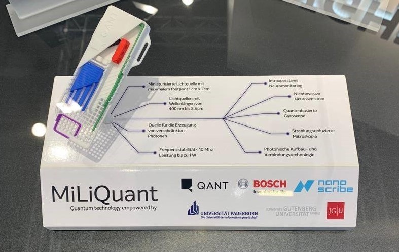
Having started in 2019, the three-year project MiLiQuant (Miniaturized light sources for industrial quantum sensors and quantum imaging systems) aims to foster new developments in quantum technologies that benefit both society and economy. In particular, the project’s research focusses on building miniaturised light sources for applications in quantum sensing and imaging. To this end, the MiLiQuant consortium comprises the companies Q.Ant, Zeiss, Bosch, and Nanoscribe, as well as the Johannes-Gutenberg-Universität Mainz and Paderborn University. The project is supported by the Federal Ministry of Education and Research (BMBF) within its funding initiative “Key components for quantum technologies” with an amount of 9.4 million Euros.
Being a collaborative project, MiLiQuant builds upon the diverse expertise of the project partners to develop light sources based on diode lasers, which are compatible with industrial quantum applications. This includes the development of sources featuring a high frequency and power stability under real world operating conditions. The target application is quantum imaging at visible and near infrared wavelengths for low light level microscopy of living cells.
In the Integrated Quantum Optics group, which is led by Prof Christine Silberhorn, we are developing tailored waveguide structures that allow for light guiding at a wavelength of 2.5µm. In addition, we investigate quantum imaging based on photon-pair correlations. This includes not only the development of the underlying theory, but also the proof-of-concept demonstration in our quantum optics’ laboratories. Within the next three years, we will transfer the scientific results into industrial applications.
Scientific contacs: Prof. Dr. Christine Silberhorn, Dr. Benjamin Brecht, Dr. Christof Eigner
The ApresSF project started in the spring of 2020 under the umbrella of the QuantERA network, which aims at strengthening quantum technologies research across Europe. The general goal of this three-year project is the development of a user friendly hard- and software platform for super-resolved time and frequency measurements.
Besides the “Integrated Quantum Optics” group of Professor Christine Silberhorn at Paderborn University, the consortium comprises workgroups from Poland, Czech Republic, Spain, and France. Led by Professor Lukasz Rudnicki from Gdansk University, ApresSF will provide innovative theory approaches and novel quantum devices that facilitate the measurement of timings and spectra with a resolution that goes far beyond anything that is possible when using classical physics only. The Paderborn research, which is led by Dr. Benjamin Brecht, will focus on designing and building the required quantum devices and performing the experiments.
Project ApresSF is supported by the BMBF under the QuantERA programme, which has received funding from the European Union's Horizon 2020 research and innovation programme.
Scientific contacs:Dr. Benjamin Brecht, Prof. Dr. Christine Silberhorn
The QuICHE project started in the spring of 2020 under the umbrella of the QuantERA network, which aims at strengthening quantum technologies research across Europe. The general goal of this three-year project is the realization of innovative high-dimensional quantum communications using time and frequency to encode information.
Besides the “Integrated Quantum Optics” group of Professor Christine Silberhorn at Paderborn University, the consortium comprises workgroups from Italy, Germany, UK, France, and Poland. Led by Professor Chiara Macchiavello from INFN Pavia, QuICHE will provide the fundament for quantum communications using large alphabets in time and frequency. Usually, information is encoded in “0” and “1” – the so-called binary encoding. It has been shown, however, that larger alphabets are beneficial for quantum communications; they can, for instance, increase the security in quantum key distribution. In QuICHE, we will devise optimised time-frequency alphabets and their experimental realisation. The Paderborn researchers under the lead of Dr. Benjamin Brecht will implement novel encoding strategies and demonstrate high-dimensional quantum key distribution with increased security and communication rates.
Project QuICHE is supported by the BMBF under the QuantERA programme, which has received funding from the European Union's Horizon 2020 research and innovation programme.
Scientific contact: Dr. Benjamin Brecht, Prof. Dr. Christine Silberhorn
More informationen:
https://www.forschung-it-sicherheit-kommunikationssysteme.de/projekte/quiche
The capability to performing measurements and evaluating these measurements in a proper way are crucial for the advance of THz communication systems. Metrology at THz frequencies is however still in its infancy and as of today it only covers detector calibration for characterization of ultrafast devices and to measurement uncertainty analysis of different spectrometer types available at THz frequencies. In the Research Unit Meteracom (Metrology for THz communication (FOR 2863)) a consortium of universities, the Physikalisch-Technische Bundesanstalt (PTB) and the National Physics Laboratory of Great Britain (NPL) addresses major challenges of THz metrology in a systematic way. Target is to establish measurement methods which are traceable to the international system of units (SI), to evaluate THz measurement devices and perform THz system measurements. In the Meteracom project, the SCT group contributes with its expertise in an ultra-low-jitter optoelectronic frequency synthesizer design. This low jitter frequency synthesizer puts the maximum data rate at higher bit rates limited theoretically by the jitter of the transceiver’s local oscillator. In addition, the SCT group develops ultra-wide-band optically-switched electronic sampler ICs as well as a new generation of optical Nyquist pulse sampler ICs in an advanced silicon photonics technology.
Website: www.meteracom.de
Scientific contact:
PhD student:
Meysam Bahmanian
Responsible for frequency synthesizer and high speed ADC design.
Email: meysam.bahmanian[at]uni-paderborn.de
Supervisor:
Christoph Scheytt
Email: christoph.scheytt[at]hni.uni-paderborn.de
Publications:
Bahmanian, Meysam; Fard, Saeed; Koppelmann, Bastian; Scheytt, Christoph: Wide-Band Frequency Synthesizer with Ultra-Low Phase Noise Using an Optical Clock Source. In: 2020 IEEE/MTT-S International Microwave Symposium (IMS), Los Angeles, CA, USA, USA, 4. - 6. Aug. 2020, IEEE (Details)
Scheytt, Christoph; Wrana, Dominik; Bahmanian, Meysam; Kallfass, Ingmar: Ultra-Low Phase Noise Frequency Synthesis for THz Communications Using Optoelectronic PLLs. In: International Workshop on mobile THZ Systems (IWMTS), 2. - 3. Jul. 2020 IWMTS (Details)
STORMYTUNE is a three-year project within the framework of the EU’s Horizon 2020 FET Open Calls. The strategic goal of STORMYTUNE is to establish quantum time and frequency measurements as upcoming quantum technology. To this end, we develop novel quantum inspired methods for the measurement of timings and spectra with a resolution that overcomes classical limitations; in addition, we design our methods such that they are user-friendly and genuinely practical, making them relevant for real-world applications.
Quantum metrology is a thriving research field. Starting as a playground for theoretical ideas, it has matured into a serious contender in the race for practical quantum technologies. First quantum gravitational sensors are at the testing stage. Quantum time and frequency measurements, however, have received little attention to date, despite their obvious applications – e.g. GPS, LIDAR, and microscopy. Led by the “Integrated Quantum Optics” group of Professor Christine Silberhorn, STORMYTUNE explores new horizons. In collaboration with partners from the UK, France, Italy, Spain, Czech Republic, and Poland, we will shift the focus from trying to use fragile quantum probe states to implementing robust quantum measurements, which provide benefits over their classical counterparts. A clever combination of quantum entanglement, advanced data processing, and tailored quantum devices will yield a toolbox for practical time and frequency measurements. Paderborn researchers under the lead of Dr Benjamin Brecht will develop these quantum devices and demonstrates their superiority in STORMYTUNE.
STORMYTUNE receives funding from the European Union’s Horizon 2020 research and innovation programme under grant agreement No 899587.
Scientific contact: Dr. Benjamin Brecht, Prof. Dr. Christine Silberhorn
In cooperation with partners from industry and research institutes, our group develops highly integrated electro-optical MIMO radar sensors for applications in the field of highly automated driving. In contrast to other sensor concepts for automated driving, such as lidar (light detection and ranging), VLC (visible light communication) or camera-based systems, radar-based systems are significantly more robust against environmental influences, such as ambient light, rain, snow, fog, etc.. Furthermore, radar systems are able to reliably detect objects even over very long distances. However, the angular resolution of even modern radar systems is currently insufficient for automatic driving.
The limiting factor in angular resolution is, among other things, the maximum area of the antenna array (antenna aperture). The larger the antenna aperture, the better the angular resolution of the radar system, i.e. smaller objects are better detected.
A major challenge here is the communication between the high-frequency radar front-ends (77 GHz radar chip with antenna) and the central station, where the transmit signals are generated and the receive signals are processed. Even at moderate frequencies of a few GHz, the maximum spacing of the antennas is limited to a few cm due to losses in the electrical lines (several dB/cm). In contrast to electrical lines, optical fibers have losses only in the range of 0.1dB/km even at very high frequencies, which makes it possible to design the spacing of the antennas to be almost arbitrarily large, allowing the angular resolution to be set almost arbitrarily fine.
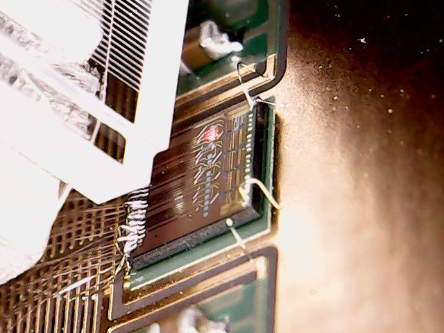
The project has developed the world's first integrated photonic-electronic radar chips. The optical signal is coupled into the chip via grating couplers, converted to an electrical signal using a photodiode and transimpedance amplifier, upconverted to the radar band of 76 GHz-77GHz, which is licensed for automotive applications, before being amplified in a buffer amplifier and a power amplifier.
Contact: Prof. Dr.-Ing. Christoph Scheytt

